How to Manage Thermal Issues in RF PCBs
Manage Thermal Issues in RF PCBs
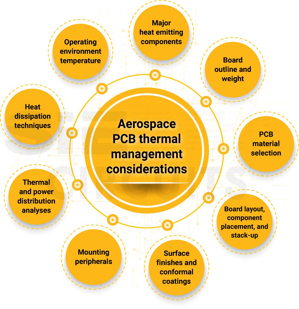
With RF PCBs, thermal issues can cause interference with signal transmission and performance lag. Achieving optimal RF performance requires careful design rules and a variety of thermal management techniques. These include selecting the right laminate materials, minimizing trace lengths and routing restrictions, proper grounding techniques, layer stack-up strategy, simulation/analysis, and manufacturing processes.
RF circuit boards have higher thermal demands than other PCBs due to their high frequencies, which require more energy from the board’s components to perform correctly. This increased electrical energy creates more heat, which raises the board’s temperature and reduces its RF performance. Thermal vias help to disperse this heat throughout the entire board, reducing its overall temperature and improving its RF performance.
A common problem that can affect RF circuit boards is signal loss and RF interference caused by signal reflection and ringing. These problems can interfere with the signal’s amplitude, causing it to lose its original waveform and resulting in poor RF performance. Using the proper copper trace width and layout, and efficient cooling techniques can help to minimize these effects.
Another important issue is the ability of rf pcb to resist thermal stress during assembly. The soldering process generates a lot of heat that can stress the RF PCB and components. To mitigate these issues, manufacturers use thermal vias in the board’s design to disperse heat and eliminate hot spots.
How to Manage Thermal Issues in RF PCBs
The material used for RF PCBs should also have good thermal properties, particularly the dielectric constant. A material’s dielectric constant is the amount of energy it absorbs at a given frequency. For RF circuits, the dielectric constant of the material should be a single value that is consistent across the operational range of the board.
Impedance matching is also essential for RF circuits, as the characteristic impedance of a copper trace decreases at higher frequencies. This can cause loss of amplitude, distortion and phase delay in the signal. To avoid these issues, designers should use a wide range of impedance-matching methods such as series or shunt impedance matching and L-section matching.
RF circuits are also more sensitive to noise, which can cause a variety of problems, including thermal, shot, phase and flicker noise. This can be mitigated by avoiding the use of parallel traces on a circuit board, and making sure to avoid routing signals near high-speed digital traces or power planes.
RF circuits are also prone to EMC (Electromagnetic Compatibility) interference, which can cause unwanted interference between the components on a circuit board. This can be caused by a variety of factors, including EMI/EMC coupling between adjacent circuits, reflected signals and electromagnetic interference from other external sources. This can be prevented by ensuring that all components on the circuit board have a consistent voltage supply and are properly grounded, as well as ensuring the proper spacing and routing of signals.